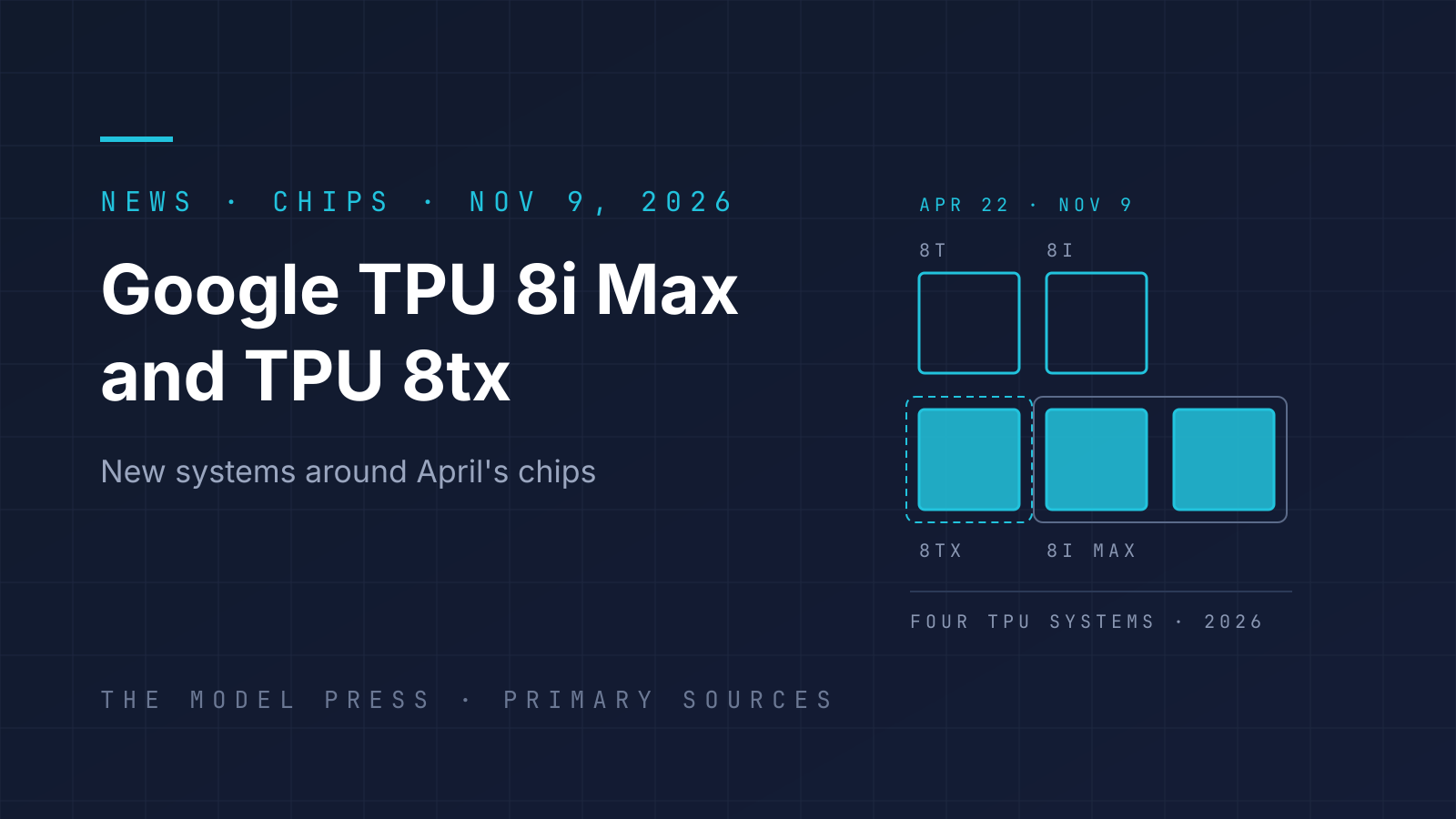
Google announced TPU 8i Max and TPU 8tx on November 9, 2026, two new systems built from the eighth-generation TPU chips it introduced in April. In its announcement, Google describes TPU 8i Max as two TPU 8i chips combined on one package for long-context work, and TPU 8tx as TPU 8t silicon paired with 5th Gen AMD EPYC host CPUs for confidential inference. It is the first time Google has introduced four TPU systems in one year.
The point Google stresses is that neither is a new chip. A new chip takes years of design and manufacturing; a new system changes what surrounds the chip (packaging, memory, network, host CPU and security) and, in Google’s words, can be delivered “in a matter of months rather than years”. The November 9 post gives no price, no availability date and no absolute specifications for either system.
On this page
TPU 8i Max: two 8i chips on one package
Google says TPU 8i Max delivers double the compute, double the on-chip SRAM and double the HBM bandwidth of TPU 8i, and fits twice the silicon in the existing rack footprint. Google aims it at what it calls the memory wall: dozens of agents working across a whole codebase or hours of video, where reading data from memory, not arithmetic, sets the pace.
Google published per-chip TPU 8i figures in its April technical deep dive. Applying Google’s “double” to them gives the TPU 8i Max column below. Those 8i Max numbers are our arithmetic on Google’s figures, not a Google spec sheet.
| Per package | TPU 8i (Google, April 22) | TPU 8i Max (2 × TPU 8i, derived) |
|---|---|---|
| Chips | 1 | 2 |
| Peak FP4 | 10.1 PFLOPS | 20.2 PFLOPS |
| On-chip SRAM | 384 MB | 768 MB |
| HBM bandwidth | 8,601 GB/s | 17,202 GB/s (about 17.2 TB/s) |
| HBM capacity | 288 GB | Not stated by Google |
One cell in that table has no number on purpose. Google’s November 9 post, its TPU product page and AMD’s release all say “double the HBM bandwidth” and none of them says “double the HBM capacity”. We checked all three on November 10, 2026. Bandwidth and capacity are different limits: bandwidth decides how fast weights and KV cache are read on every decoding step, capacity decides how large a model and context fit at all. Until Google publishes a capacity figure for TPU 8i Max, 576 GB (2 × 288 GB) is an assumption, not a spec.
TPU 8tx: TPU 8t silicon, AMD hosts, the 8i network
TPU 8tx changes three things around the TPU 8t chip, and each one is visible against the April spec table.
| TPU 8t (April) | TPU 8tx (November 9) | |
|---|---|---|
| Silicon | TPU 8t | Same silicon as TPU 8t |
| Host CPU | Google Axion (Arm) | 5th Gen AMD EPYC (x86) |
| Chip-to-chip network | 3D torus, 9,600 chips per superpod | Boardfly, the low-latency topology of TPU 8i |
| Main job | Large-scale pre-training | Confidential inference and small-scale training |
| Latency claim | Baseline | Up to 2x lower than TPU 8t, as Google states it |
The host change is the notable one. In April, Google said it had moved its whole eighth generation onto its own Arm-based Axion CPUs. TPU 8tx is the exception, and the reason is security: AMD’s November 9 release says the system uses AMD Secure Encrypted Virtualization (SEV) on the EPYC host, together with the TPU, to extend confidential computing from the CPU to the attached accelerators. The accelerator’s identity and security configuration are verified before it gets direct access to protected memory, so prompts, model weights and intermediate data stay encrypted in CPU memory and in transit between host and accelerator. AMD and Google call TPU 8tx the first cloud TPU system with hardware-enforced confidential computing.
Google pitches the system at regulated enterprises and governments, and says teams can fine-tune on private data, distill large models into smaller ones and run reinforcement learning on the same system without moving sensitive data between clusters. Google claims the protection costs “near-zero” performance. Neither company has published a measurement behind that claim or behind the 2x latency figure.
Bandwidth per unit of compute, from Google’s own numbers
Dividing Google’s April figures shows why TPU 8i, not 8t, is the base for a long-context system:
| Ratio (our arithmetic) | TPU 8t | TPU 8i and TPU 8i Max |
|---|---|---|
| HBM bandwidth per FP4 PFLOP | 518 GB/s | 852 GB/s |
| On-chip SRAM per FP4 PFLOP | 10.2 MB | 38.0 MB |
| Time to read the full HBM once | 33.1 ms (216 GB at 6,528 GB/s) | 33.5 ms for TPU 8i (288 GB at 8,601 GB/s) |
TPU 8i carries about 1.6 times as much memory bandwidth per unit of compute as TPU 8t, and nearly four times as much SRAM per unit of compute. Because TPU 8i Max doubles compute, SRAM and bandwidth together, those ratios stay the same; what grows is the amount of each per package and per rack. That fits Google’s description: TPU 8i Max is about density, not a different balance of memory and math.
The last row gives a useful bound for decoding. When a model’s weights and KV cache fill the HBM, each generated token has to stream that data through the chip at least once, and at the published bandwidth one full pass takes about 33 milliseconds on either chip. That is a ceiling of roughly 30 decoding steps per second for a workload that fills the whole memory, before any other overhead; smaller working sets, and data held in SRAM, go faster. Our KV cache explainer covers why decoding is bound by memory reads, and the HBM memory explainer covers the memory itself.
The software Google announced alongside
The same post lists software changes that apply across the TPU line:
- Cloud Pathways, the single-controller runtime Google DeepMind uses for Gemini, is now generally available on Google Kubernetes Engine.
- GKE dynamic slicing is generally available. It assembles or splits TPU topologies through optical circuit switches; Google says job start-up is up to 5x faster and fault recovery up to 4.5x faster.
- TPU Sync, which Google calls a model-state layer that tiers KV cache across HBM, host DRAM and storage, is being open-sourced. Google claims it cuts KV transfer latency and time to first token by more than 90%.
- An open-source TPU agent suite for coding tools is in preview, and an open-source XLA Serving Engine was announced. Google says it open-sourced TorchTPU in October; we covered its vLLM and SGLang engines for TPU on October 20.
Google also says TPUs now have “nearly 100 customers” and that customers can deploy TPUs directly in their own data centers.
Where the eighth generation stands
| System | Announced | What Google says it is for | Availability as Google states it |
|---|---|---|---|
| TPU 8t | April 22, 2026 | Large-scale pre-training | “Later this year” (April 22) |
| TPU 8i | April 22, 2026 | Low-latency inference and reasoning | “Later this year” (April 22) |
| TPU 8tx | November 9, 2026 | Confidential inference, small-scale training | No date given |
| TPU 8i Max | November 9, 2026 | Massive context windows, rack density | No date given |
The April figures for both chips are in our AI chips catalog: TPU 8t, TPU 8i and the previous-generation Ironwood, alongside other vendors in the AI chips table. How the TPU line developed and who can use it is in our Google TPU explainer.